

Chiplet architecture is changing electronics packaging by splitting one large chip into several smaller dies that work together in one package. It is already used in modern CPUs and advanced packaging platforms from AMD and Intel.
A chiplet architecture paper usually focuses on interconnects, packaging, and system integration because those parts decide performance, power use, cost, yield, and long term scalability.
What Chiplet Architecture Changes in Packaging
Chiplet design moves hardware away from one very large monolithic die and toward smaller dies that are combined in a single package. This approach helps teams mix different process nodes in one product, such as advanced logic on a leading edge node and I/O or memory support on a mature node. AMD describes its chiplet strategy as a way to add more CPU cores by combining chiplets in a package, while Intel describes Foveros 2.5D as a way to place multiple chiplets together with better density and lower wire parasitics.
This change matters because packaging is no longer a simple support layer. It becomes part of the main system design. The package now carries more of the job of interconnect, signal integrity, thermal behavior, and product scaling. Academic reviews of chiplet systems also note that chiplets improve integration and performance, but they raise new demands in interface design, packaging quality, and standards.
Why the Research Paper Matters
A chiplet architecture paper is important because it explains the tradeoffs that hardware teams must manage. The MDPI review on chiplet heterogeneous integration shows that chiplets promise better cost control, faster development, and stronger system flexibility, but they also create challenges in interconnect standards, packaging technology, and quality control.
That research direction is now visible in industry. AMD’s 2024 chiplet white paper says it covers chiplet advantages, challenges, integration, the ecosystem, and the role of UCIe. Intel’s packaging briefs explain how Foveros and EMIB support complex chip designs, while the UCIe consortium positions open chiplet standards as the base for an open ecosystem.
Main Hardware Impact
Chiplet packaging changes modern hardware in four clear ways. It can improve yield by making each die smaller. It can reduce cost by letting teams use the best process node only where it matters most. It can improve performance by shortening some internal connections inside the package. It can also make product lines more scalable because manufacturers can combine different chiplet counts or different chip types in one family. AMD and Intel both describe these benefits in their public architecture and packaging documents.
At the same time, chiplets make the package more complex. The links between chiplets must be fast, low power, and reliable. The 2020 review paper notes that the biggest challenges are interconnect interfaces, protocols, packaging technology, and quality control. It also states that bandwidth per area and power per bit are central design goals.
Monolithic Versus Chiplet Packaging
| Area | Monolithic design | Chiplet design | Hardware impact |
|---|---|---|---|
| Die size | One large die | Several smaller dies | Smaller dies can improve yield and make scaling easier. |
| Process nodes | Usually one node for most functions | Different dies can use different nodes | High performance logic and lower cost I/O can live in the same package. |
| Interconnect | Mostly on die wiring | Die to die links matter more | Packaging becomes a performance driver, not just a support layer. |
| Product scaling | Harder to expand without redesigning the whole die | Easier to build different versions from the same blocks | Vendors can create more product tiers from shared chiplets. |
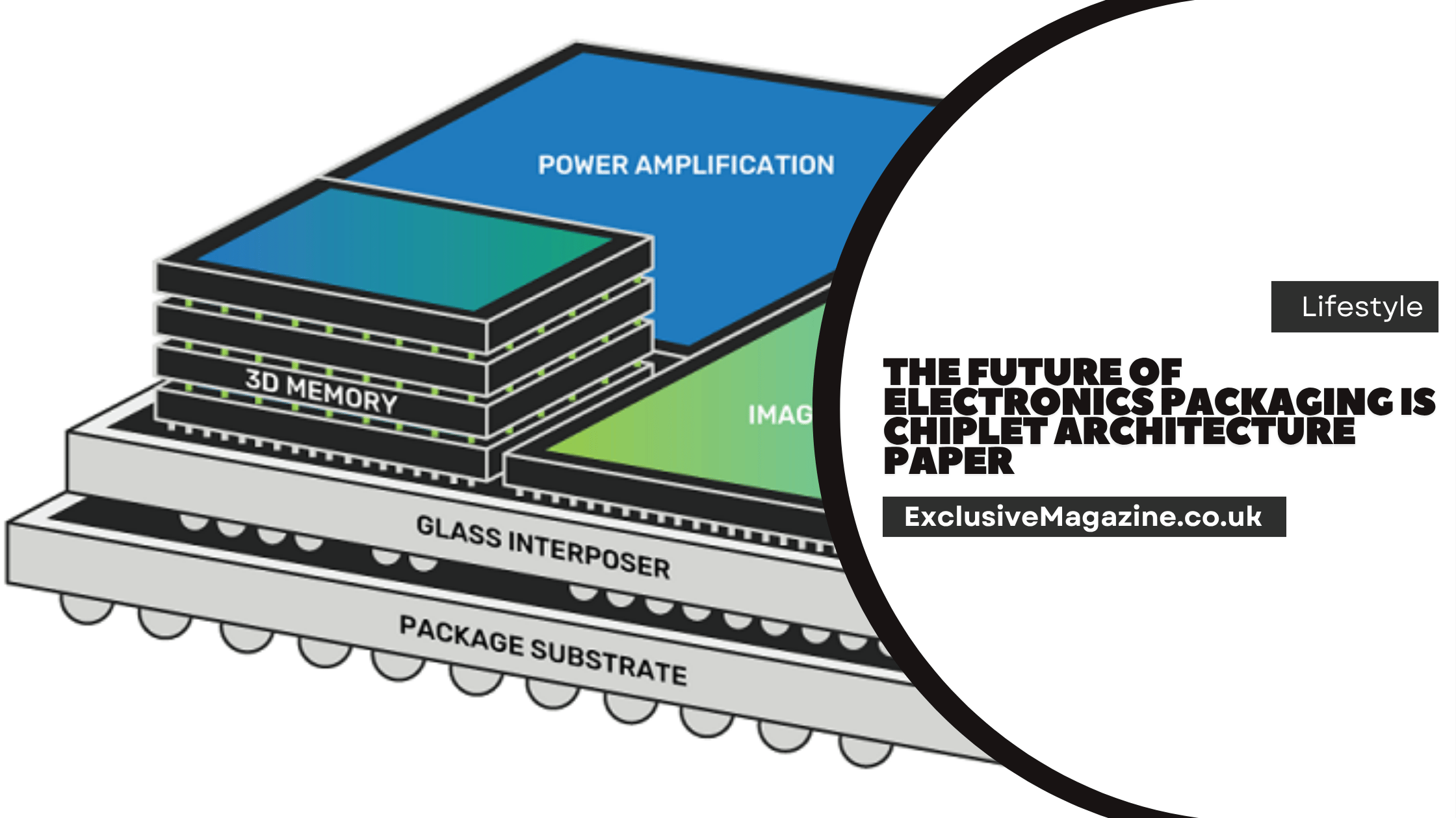
Packaging Technologies That Support Chiplets
Modern chiplet systems use more than one packaging method. Intel’s Foveros 2.5D uses die stacking and a passive base die with active dies on top. Intel says this improves die density, reduces package footprint, and allows advanced nodes and mature nodes to be combined more cost effectively. Intel also says Foveros uses face to face bonding with very fine microbump pitch to improve interconnect density.
Intel’s EMIB technology adds another path. Intel explains that EMIB creates high bandwidth connectivity between multiple large chiplets without using a silicon interposer. Intel also says EMIB can be combined with Foveros to form EMIB 3.5D, which is designed for flexible, heterogeneous systems and a much larger total silicon surface area inside one package.
The academic literature describes the same packaging split in a broader way. It groups chiplet packaging into substrate based packaging, silicon interposer based packaging, silicon bridge based packaging, and RDL based fan out packaging. It also notes the tradeoff clearly. Organic substrates are cheaper, while silicon interposers usually deliver higher I O density and lower delay and power, but at higher process cost.
Role of Open Standards
Open standards are now central to chiplet packaging. The UCIe consortium says its goal is to build an open ecosystem of chiplets for on package innovation, and it says the UCIe 3.0 specification is now part of that effort. Intel also states that its Foveros packaging portfolio is compatible with UCIe and that UCIe helps enable high density integration of chips from different sources. AMD’s 2024 white paper also discusses the role of UCIe in chiplet integration.
This matters for modern hardware because a shared interconnect reduces the risk that every vendor builds a private, closed package language. When the physical and protocol layers become more standard, designers can mix IP blocks more easily and focus on product goals instead of building every die link from scratch. That is one of the main reasons chiplets are now a serious part of system level hardware planning.
Impact on CPUs, Servers, and AI Hardware
In CPUs and servers, chiplets help manufacturers scale core counts and build product ranges more efficiently. AMD says its chiplet strategy lets more chiplets be added to a package to create a higher performance processor. AMD also says its hybrid multi chip architecture helps decouple innovation paths and deliver high performance products.
This design approach is especially useful for data center hardware. Intel’s packaging brief says EMIB 3.5D can combine compute modules with I O tiles or DRAM modules, which is important for flexible heterogeneous systems. That kind of packaging is relevant to AI and HPC products because those workloads need large memory bandwidth, strong compute density, and careful power control.
Chiplets also help when different blocks do not need the same transistor density. A modern package may need high end logic, memory support, analog functions, and I O in one design. The chiplet model makes that practical by placing each function on the most suitable die. Intel explicitly says active dies can be logic, memory, or FPGA blocks, and the MDPI review notes that chiplets support heterogeneous integration of different functional blocks.
Education platforms such as the fintechzoom.io stock market course also reflect the growing need for structured learning in advanced technology sectors, where semiconductor trends and hardware innovation are increasingly tied to financial and market understanding.
Design and Manufacturing Effects
Chiplet architecture changes how companies build hardware. It reduces dependence on a single giant die, which can help with yield and can lower the cost of failed wafers. It also changes the supply chain because packaging, testing, and interconnect validation become more important than before. The research literature says these gains are real, but it also warns that the ecosystem needs better standards, better packaging, and better quality control before chiplets become fully mature across all device classes.
The paper level view is useful here because it shows that chiplets are not only a hardware idea. They are also a systems idea. A strong chiplet design must match package physics, electrical limits, thermal behavior, protocol choice, and product planning. That is why chiplet architecture now sits at the center of advanced electronics packaging instead of at the edge of it.
A similar shift in ownership and structure can be seen in how tech consulting majority stake financial sponsor today deals are shaping modern technology companies, especially where strategic investors influence long term engineering and infrastructure decisions.


